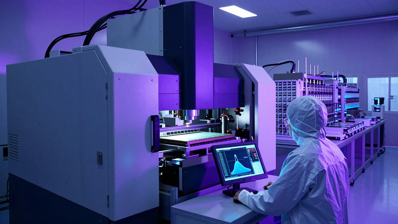

TSMC Investment Readiness Calculator
Configure Region Parameters
Adjust the sliders to simulate different regional conditions. A score above 80 is typically required for advanced wafer fabs.
Investment Analysis
--
Readiness Score (0-100)
Awaiting Analysis
Adjust parameters and click analyze to see if the region is ready for a TSMC-style advanced wafer fab.
For years, the Indian government has aggressively courted TSMC, the world’s largest pure-play semiconductor manufacturer. The goal is clear: integrate India into the global semiconductor value chain to reduce dependence on China and boost domestic manufacturing. Yet, as of mid-2026, there is no major operational wafer fab from TSMC on Indian soil. While other giants like Micron have moved forward with assembly and testing facilities, the crown jewel of advanced chipmaking remains elusive for New Delhi. Why? It isn’t just one factor; it’s a complex web of infrastructure deficits, geopolitical caution, and economic realities that make India a high-risk, long-term bet compared to established hubs.
The Scale of Capital and Infrastructure Demands
Building a semiconductor fabrication plant (fab) is not like setting up a textile mill or an automobile assembly line. A modern advanced-node fab costs between $15 billion and $20 billion to build. This is capital-intensive beyond most national budgets, let alone private corporate balance sheets without significant state subsidies. For TSMC, every dollar spent must yield a return through volume and efficiency. In Taiwan, they benefit from decades of accumulated infrastructure. In India, the foundational requirements are still being built.
The most critical bottleneck is water. Semiconductor manufacturing is incredibly thirsty. Producing a single batch of wafers requires thousands of liters of ultra-pure water. Many potential sites in India face chronic water scarcity or inconsistent supply chains. Unlike in Arizona or Singapore, where water management systems are mature and heavily subsidized for tech parks, Indian states often struggle to guarantee the continuous, high-volume water supply needed for 24/7 operations. If a fab stops production for even a few hours due to a power or water glitch, the financial loss runs into millions of dollars instantly.
Then there is electricity. Chip fabs require uninterrupted, stable power with zero voltage fluctuations. Grid instability in parts of India remains a concern. While renewable energy targets are ambitious, the baseload reliability required for sensitive lithography machines is hard to guarantee without massive investment in dedicated microgrids and backup systems. TSMC needs certainty, and right now, India offers potential rather than proven reliability at scale.
The Ecosystem Gap: More Than Just Silicon
Semiconductor manufacturing doesn’t happen in a vacuum. It relies on a dense ecosystem of suppliers, skilled labor, and specialized logistics. In Taiwan, you can find a supplier for photoresist chemicals, precision lenses, or gas purification systems within a two-hour drive. This proximity reduces lead times and allows for rapid troubleshooting. In India, this ecosystem is virtually non-existent for advanced nodes.
If a machine breaks down in an Indian fab, engineers might need to fly in specialists from Europe or Asia, causing delays that cost billions in lost output. TSMC’s competitive advantage lies in its ability to iterate quickly. Without a local cluster of suppliers for materials like silicon wafers, specialty gases, and packaging substrates, the supply chain becomes fragile. Importing these materials adds cost and time, eroding the margin benefits of lower labor costs in India.
Furthermore, the talent pool, while large, lacks specific depth. India produces millions of engineering graduates annually, but the number of professionals with hands-on experience in nanometer-scale fabrication is tiny. Most experienced semiconductor engineers are concentrated in the US, Taiwan, South Korea, and Japan. Training a workforce from scratch takes years, during which productivity will be low. TSMC prefers locations where they can plug into an existing talent network rather than building one from the ground up.

Geopolitical Calculations and Risk Diversification
Geopolitics plays a massive role in TSMC’s strategy. The company is under immense pressure from Washington to diversify away from Taiwan due to fears of Chinese aggression. This led to investments in Arizona, USA, and discussions about Japan and Germany. These locations offer political stability, strong IP protection laws, and closer alignment with Western security interests.
India, while strategically important as a counterweight to China, presents different risks. Its foreign policy is non-aligned, meaning it maintains strong trade ties with Beijing. For a company like TSMC, navigating the dual pressures of pleasing Washington while maintaining business relations with China is delicate. Investing heavily in India could complicate this balance. Additionally, regulatory unpredictability in emerging markets is a red flag for investors. Changes in tax laws, import duties, or land acquisition policies can happen overnight, threatening long-term ROI.
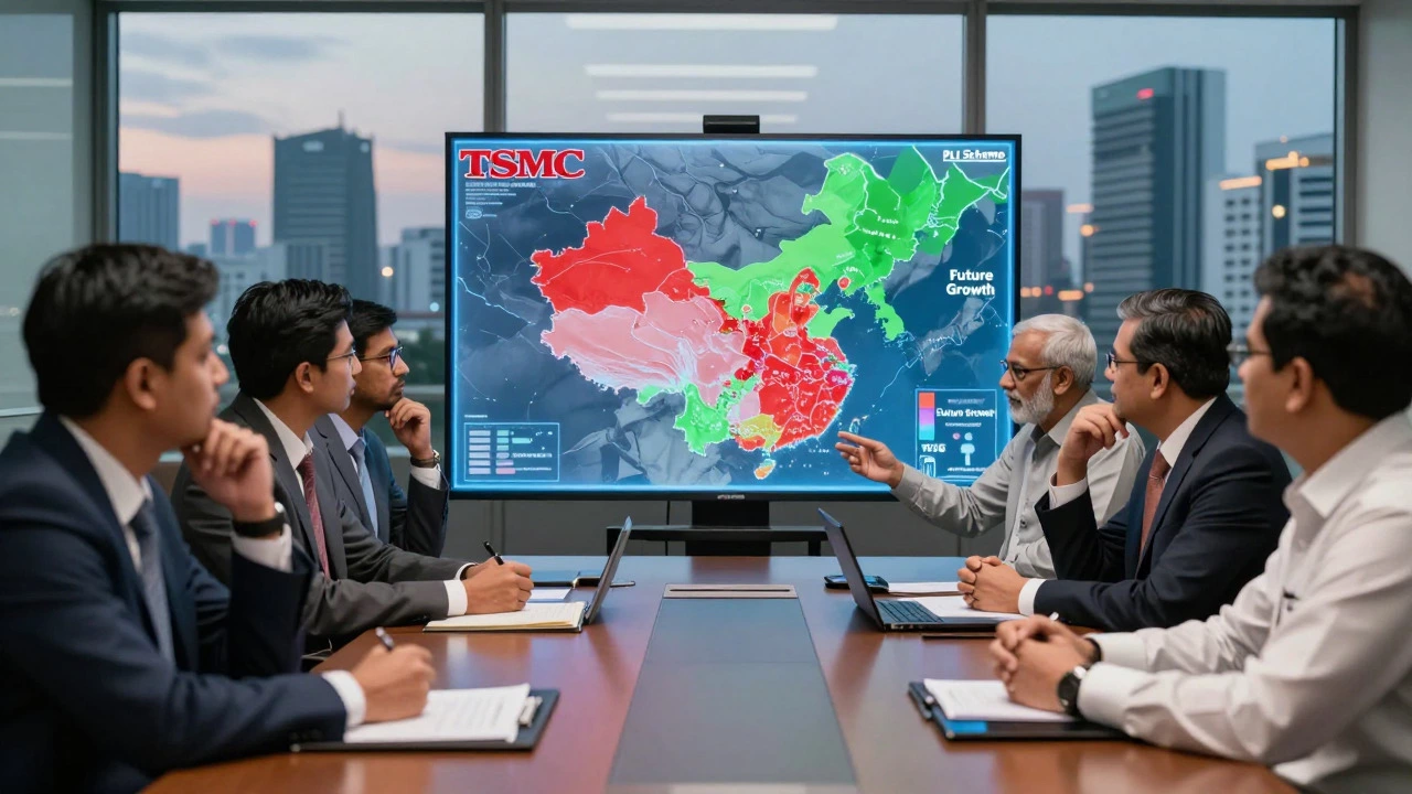
TSMC’s current expansion strategy focuses on "friend-shoring" to allies with established rule-of-law frameworks. The US CHIPS Act provides direct grants and loans, reducing financial risk. Japan and Germany offer similar incentives with less bureaucratic friction. India’s Production Linked Incentive (PLI) scheme is attractive, but it is primarily designed for back-end operations like assembly, testing, and packaging (ATP), not front-end wafer fabrication. The PLI caps subsidies at levels that may not fully offset the higher initial setup costs and operational inefficiencies in a new market.
The Competition for Global Foundry Capacity
TSMC is not the only player in town. Samsung, Intel, and GlobalFoundries are also expanding globally. However, none have committed to full-scale advanced wafer fabs in India yet. Instead, they are focusing on older nodes or packaging technologies. This signals a broader industry consensus: India is ready for the lower end of the semiconductor chain, but not yet for the cutting edge.
Consider the case of Micron Technology. They announced a $2 billion investment in Gujarat for ATP facilities. This is a logical first step. ATP plants require less extreme environmental controls, use less water, and rely more on manual labor, which India has in abundance. By starting here, companies can test the waters, build local partnerships, and train workers without the existential risk of a $20 billion wafer fab. TSMC likely sees this same path: wait for the ecosystem to mature through ATP growth before committing to front-end manufacturing.
| Factor | Taiwan / US | India (Current Status) |
|---|---|---|
| Infrastructure | Mature, reliable power/water grids | Developing, regional inconsistencies |
| Ecosystem | Dense supplier network, short lead times | Limited local suppliers, heavy imports |
| Talent Pool | Deep expertise in advanced nodes | Large general engineering base, niche gap |
| Subsidies | High (CHIPS Act, etc.) | Moderate (PLI Scheme) |
| Political Risk | Low (Allied nations) | Moderate (Regulatory changes) |
The Path Forward: What Needs to Change?
Does this mean TSMC will never invest in India? Not necessarily. The trajectory is positive, but the timeline is longer than politicians hope. For TSMC to consider a greenfield fab, several conditions must be met. First, India must demonstrate successful operation of multiple ATP plants and older-node fabs by other players. This proves the market viability and operational feasibility.
Second, infrastructure upgrades must accelerate. Dedicated industrial corridors with guaranteed water recycling plants and independent power projects are essential. Third, education reform is crucial. Universities need to partner with industry to create specialized curricula in semiconductor physics and materials science. Scholarships and training programs funded by the government can help bridge the skills gap faster.
Finally, policy stability is key. Long-term guarantees on tax holidays, land rights, and import duties for raw materials would give TSMC the confidence to lock in multi-decade investments. The recent push by the Indian government to establish a Semiconductor Mission is a step in the right direction, but execution matters more than announcements.
Conclusion: Patience Over Pressure
The absence of TSMC in India is not a rejection of the country’s potential, but a reflection of current realities. Semiconductor manufacturing is the pinnacle of industrial complexity. It demands perfection in infrastructure, supply chain, and human capital. India is building these foundations, but it takes time. As the global supply chain reshuffles post-pandemic, India’s role will grow. But until the ecosystem matures, TSMC will likely stick to safer bets in allied nations, watching India’s progress from the sidelines, ready to jump in when the risk-reward ratio finally aligns.
Will TSMC ever open a factory in India?
It is possible, but unlikely in the short term (next 3-5 years). TSMC is currently focused on expansions in the US, Japan, and Germany. India may see TSMC involvement later if the local ecosystem for advanced node manufacturing matures significantly and infrastructure risks are mitigated.
What is the difference between wafer fabrication and ATP?
Wafer fabrication (front-end) involves creating the actual chips using complex lithography processes requiring cleanrooms and expensive equipment. Assembly, Testing, and Packaging (ATP, or back-end) involves putting the finished chips into protective casings and testing them. ATP is less capital-intensive and more labor-heavy, making it a better fit for India's current capabilities.
Why does water matter so much for chip factories?
Water is used to clean silicon wafers at every stage of production. Even microscopic particles can ruin a batch. Fabs need thousands of liters of ultra-pure water daily. Any interruption in supply stops production immediately, leading to massive financial losses.
Which countries are competing with India for semiconductor investment?
The United States, Japan, Germany, and Malaysia are actively competing. The US offers the CHIPS Act subsidies, Japan and Germany provide strategic EU/Asian alliances, and Malaysia has an established semiconductor history. These regions offer more immediate infrastructure readiness than India.
What is India's PLI scheme for semiconductors?
The Production Linked Incentive (PLI) scheme offers financial incentives to companies that set up manufacturing units in India. For semiconductors, it covers design, fabrication, and ATP. However, the incentive rates are capped, which may not fully cover the high initial costs of advanced wafer fabs.